Why PCAL6524 is a Widely Capable IO Expander
PCAL6524 from NXP is an ultra low-voltage, level translating, 24-bit I/O, fast mode plus (FM+) capable, I2C / SMBus I/O expander with Agile I/O features, external interrupt output, and external reset pin.
This device comes in two flavors for packaging.
The HUQFN32 package is 5 mm x 5mm x 0.56 mm.
The VFBGA36 is a 2.6 mm x 2.6 mm ball grid array package.
This is a widely capable device one for its extensive list of features, small package sizing, and its ability to operate at 1 MHz I2C. Let’s review the major features of this device:
Voltage Supply + Level Translation:
This device has two supplies.
VDD(I2C-bus): 0.8 V to 3.6 V
VDD(P): 1.65 V to 5.5 V
Level translation can occur between the I2C pins and I/O pins.
24-bit:
The device has 24 configurable I/O pins across 3, 8-bit ports.
Fast Mode+:
The device can operate in the three standardized modes of I2C.
Standard Mode: 0 to 100 kHz
Fast Mode: 0 to 400 kHz
Fast Mode+: 0 to 1 MHz
Low Standby Current:
The PCAL6524 can read a standby current all the way down to 3 uA in the idle state.
5.5 V Tolerant I/O Ports:
The I/O pins are 5.5 V tolerant. If the VDD(P) supply voltage is 3.3 V, the I/O’s can tolerate an over voltage signal up to 5.5 V.
/RESET and /INT:
PCAL6524 provides external active LOW /RESET and active LOW open-drain interrupt output.
HBM and CDM JESD22 Specs:
Human Body Model - HBM = +/- 2 kV
Charged Device Model - CDM = +/- 1 kV
I2C Device Address Selection:
The PCAL6524 has 4 device address selections by configuring the ADDR pin to either SCL / SDA / VSS / VDD.
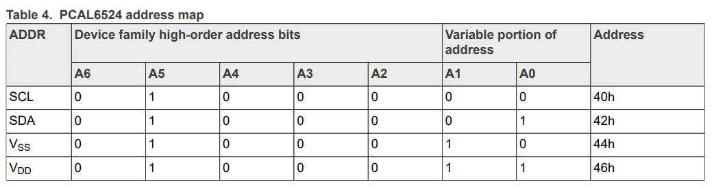
Table 4 - PCAL6524 Address Map - Page 7
Software Reset Call and Device ID:
The PCAL6524 can be reset through the external /RESET pin or through a software reset sequence in-band the I2C bus.
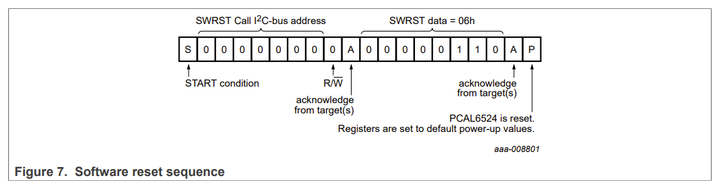
Figure 7 - Software Reset Sequence - Page 8
PCAL6524 can also be identified through the I2C bus through its device ID.
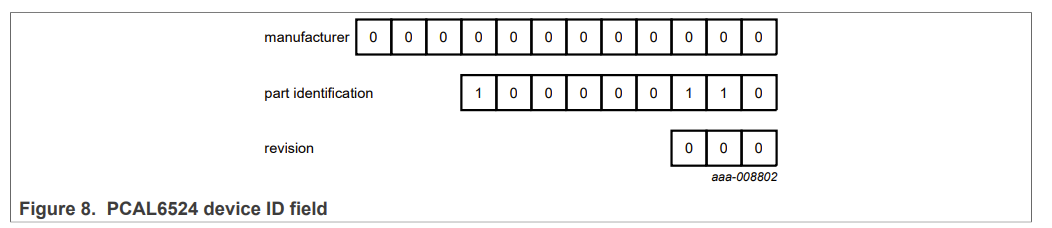
Figure 8 - Device ID Field - Page 8
Input Port Register (0x00 - 0x02):
This register is used to read signal inputs to the IO expander.
Output Port Register (0x04 - 0x06):
This register sets the output logic of the IO’s which are configured as OUTPUT through the configuration register (0x0C - 0x0E).
Polarity Inversion Register (0x08 - 0x0A):
The polarity inversion register flips the incoming input signal polarity, or flips the output logic polarity.
Configuration Register (0x0C - 0x0E):
The configuration register is used to set the IO’s as either INPUT or OUTPUT. A mixture of inputs and outputs can exist on the same port.
Output Drive Strength Register (0x40 - 0x45):
The output drive strength register configures the strength of an IO configured to OUTPUT. See the simplified output stage diagram:
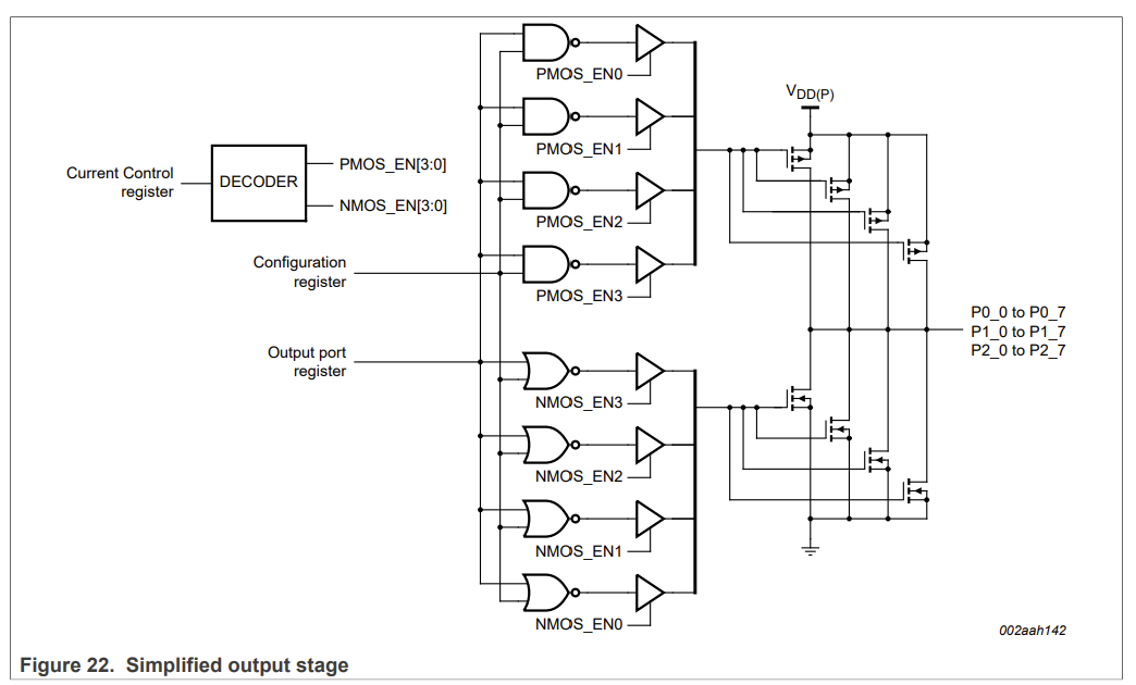
Figure 22 - Simplified Output Stage - Page 32
The four push-pull “fingers” contribute to 1/4 of the total drive strength. When all four pairs of push-pull outputs are enabled, the pin operates at full strength. This is configurable through the register.
Input Latch Register (0x48 - 0x4A):
The input latch register only affects IO’s configured as inputs.
If a state change occurs on an input pin, this will trigger an interrupt on /INT (high to low). If the same pin reverts back to its original logic state, the interrupt on /INT will de-assert (low back to high). The interrupt is lost.
If the input latch register is enabled for this input pin, then the same will occur: a state change causes an interrupt to occur on /INT. However, if the input pin reverts back to its original state, the /INT pin will stay asserted —> The interrupt is not lost!
Pull-up/Pull-down EN Register (0x4C - 0x4E):
This register enables the selected pull-up or pull-down register to the IO.
Pull-up/Pull-down Selection Register (0x50 - 0x52):
This register selects a 100k pull-up or 100k pull-down resistor for the IO pin.
Interrupt Mask Register (0x54 - 0x56):
This register will mask interrupts for specific IO’s configured as inputs. A state change on an input pin will not trigger an interrupt on /INT (i.e. the interrupt is masked).
Interrupt Edge Register (0x60 - 0x65):
The interrupt edge register sets the specific way an interrupt is asserted for the IO pins configured as inputs.
You can select rising edge triggered, falling edge triggered, or both edge triggered through this register.
Interrupt Clear Register (0x68 - 0x6A):
This register can be used to clear the interrupt source.
Input Status Register (0x6C - 0x6E):
This register is used to detect which pin(s) caused the interrupt on /INT.
Individual Pin Output Configuration Register (0x70 - 0x72):
This register can be used to set the individual output pin configuration as open-drain or push-pull. A mixture of open-drain and push-pull outputs can exist on the same port.
Switch Debounce EN Register (0x74 - 0x75):
This register enables debouncing circuitry on the IO pin.

Figure 13 - Debounce Diagram - Page 27
Switch Debounce Count Register (0x76):
The debounce count register sets the debounce counter - the time delay before sampling the input after the edge is detected. This is done through a combination of the register setting and the external oscillator at the input P0_0.
See page 27 of the datasheet for more detailed explanation.