How to Write and Read Registers within TCAL6416 IO Expander
TCAL6416 I2C IO Expander is like any I2C target. It has a device address (target address) and several register addresses known as “command bytes” in the digital core of the device.
The device address (target address) is different from a register address. You can think of the target address as referring to the TCAL6416 IO expander itself. The register address refers to the contents and configurations inside the TCAL6416.

I2C Device Address - Page 25/55 of the TCAL6416 Datasheet
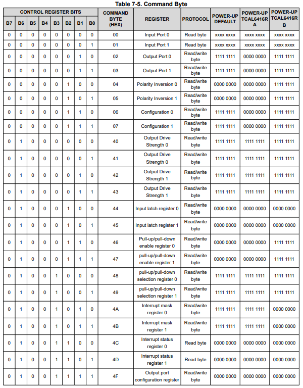
Complete Command Byte Table 7-5 on page 26/55 of the TCAL6416 Datasheet
In order to talk to the TCAL6416, you would need to send address 0x20 or 0x21 since these are the two address combinations provided by the IC.
In order to change the configuration of the IO expander, you would need to talk to a specific register inside the TCAL6416. For example, if you wanted to change the output drive strength on port 0, you would send register address 0x40 or 0x41.
Example Write:
Writing to the TCAL6416 IO expander can be found in the example on page 30 of the datasheet in figure 7-9.
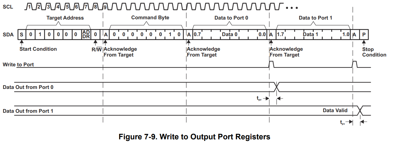
Figure 7-9 Write to Output Port Registers
Figure 7-9 walks through an example of writing data to the output port 0 register (P07 - P00) and output port 1 register (P17 - P10). This shows how to set the output logic of all 16 GPIO’s that are configured as an OUTPUT.
The following is the bit by bit description of what is being written:
Start Condition (S) - From Controller
Target (Device) Address - 0x20 or 0x21 (depending on ADDR bit)
Write Bit (0)
ACK - Comes from the Target Device
Command Byte Address (0x02 = 0b0000010) - this points to the output port register 0 from the command byte table 7-5 on page 26 of the datasheet
ACK - Comes from the Target Device
Data to Output Port 0 - this is the data that sets the output logic high or low on the Pxx output pins (P07 - P00)
ACK - Comes from the Target Device
Data to Output Port 1 - this is the data that sets the output logic high or low on the Pxx output pins (P17 - P10)
Stop Condition (P) - From Controller
Example Read:
The example read command comes from figure 7-11 on page 31 of the datasheet.
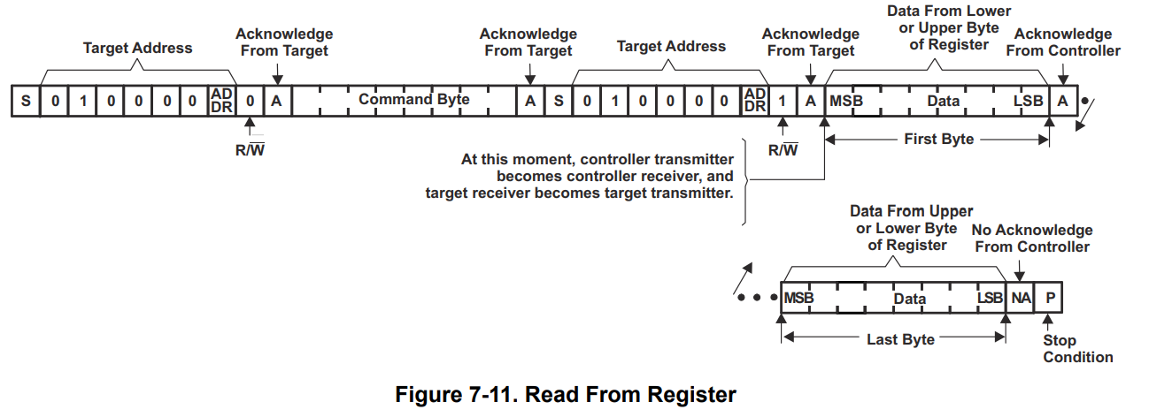
Figure 7-11 Read From Register on page 31 of the TCAL6416 Datasheet
The following is the bit by bit description of how a read transaction works:
Start Condition (S) - From Controller
Target (Device) Address - 0x20 or 0x21 (depending on ADDR bit)
Write Bit (0) - This is a “0” because we need to first set the command byte address (pointer address) we want to read data from
ACK - Comes from the Target Device
Command Byte Address From Table 7-5
ACK - Comes from the Target Device
Repeated Start (S or Sr)
Target (Device) Address - 0x20 or 0x21 (depending on ADDR bit) - must send target address again
Read Bit (1) - Since we set the command byte (pointer address) with a write bit, we now want to read from the target address so we can read data from the command byte register address.
ACK - Comes from the Target Device
Data (MSB to LSB) - this is the data read from the command byte address
ACK - Come from the Controller Device
the Controller can continue to read repeated data from the register address until a NACK is issued by the controller
NACK - Comes from the Controller Device - tells the TCAL6416 to stop data read
Stop Condition (P) - From Controller