What is Rise-Time and Fall-Time?
Rise time is defined as the time it takes for a signal to transition from a “low-level” to a “high-level.”
Likewise, fall time is the time it takes for a signal to transition from a “high-level” to a “low-level.”
Rise time and fall time can be arbitrarily defined depending on the electrical specification, datasheet, or electrical standard. Consider the rise-time and fall-time specifications from the I2C standard defined by NXP.

tr = rise-time; is from 30% to 70% of VCC
tf = fall-time; is from 70% to 30% of VCC
Page 45 / 62 - NXP I2C Standard UM10204
The USB 2.0 specification also defines rise-time and fall-time. We can see that the USB 2.0 spec defines it from 10% to 90%.

Page 180/650 of the USB 2.0 Specification
Rise-Time (THSR) is from 10% to 90%
Fall-Time (THSF) is from 90% to 10%
Why Care?
Consider this example where data is sampled on the rising edge of the clock signal.
Once the clock reaches 50% of the supply voltage VCC, it will begin to sample the data.
Data is considered a valid logic HIGH (1) if the data is above 70% of the supply voltage VCC.
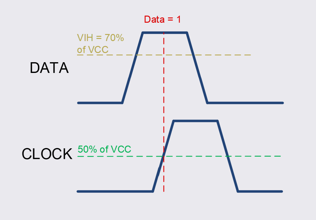
Correct data sampling, clock samples a logic HIGH “1” from the data line.
Consider in the next example that significant bus capacitance has been added to the system (most likely through parasitic capacitance such as a long trace on a PCB). The rise-time is much slower, so much so that the clock samples the data before it reaches a valid logic high signal.
In this case the data is “indeterminate.” The data is neither HIGH (1) or LOW (0). Because the rise-time is too slow, the data does not rise above a VIH in time before the clock begins the sampling process. Therefore, data is corrupted.
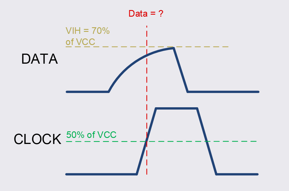
Incorrect data sampling, clock begins sampling data before a VIH, the logic could be “1” or “0” in this case.