What is a Buffered Output LOW from an I2C Buffer?
Any I2C buffer has a buffered output low voltage known as a VOL. For some buffers, the output voltage varies with its input voltage. For others, the output voltage is static or fixed output.
An example of a buffer with a fixed output voltage is the TCA9617B. If we analyze the electrical characteristics in the datasheet on page 5/28, section 5.5 Electrical Characteristics, we can see the specs for VOLA and VOLB. This is the output voltage on A-side and output voltage on B-side respectively.

VOL for SDAB/SCLB/SDAA/SCLA
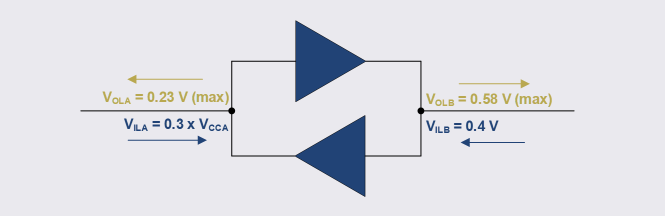
If we look at the table, we are given a couple of voltage outputs. TCA9617B is a level translating I2C buffer, so it has two outputs — depending on which side the input is driven. If you drive an input LOW on A-side, your output is VOLB. If you drive an input on B-side, your output is VOLA.
If we look at VOL on SDAB or SCLB, this is the output low voltage for both pins. The output drive structure is the same on the data line and clock line. With an input of VILA = 0V, i.e. you pull the A-side input to GND level, and you sink a current of 100 uA or 30 mA on B-side (IOL), you can expect your VOL (b-side) voltage to be within 0.48 V to 0.58 V with 0.53 V being the typical value. This is also across voltage too. Your VCC supply voltage can be anywhere from 2.2 V to 5.5 V.
This ultimately means that your output voltage on B-side does not change much with respect to your supply voltage or output current load on B-side. You could be drawing 100 uA out of B-side with VCC = 2.2 V, and you can still expect your output voltage to be near 0.53 V.
For A-side, VOL on SDAA or SCLA when drawing IOLA = 30 mA is typical 0.1 V, or 0.23 V max.
To understand why B-side output voltage VOLB is much higher than A-side, we need to understand the VILB spec (input low voltage on B-side). Below is the VILB spec in the datasheet.
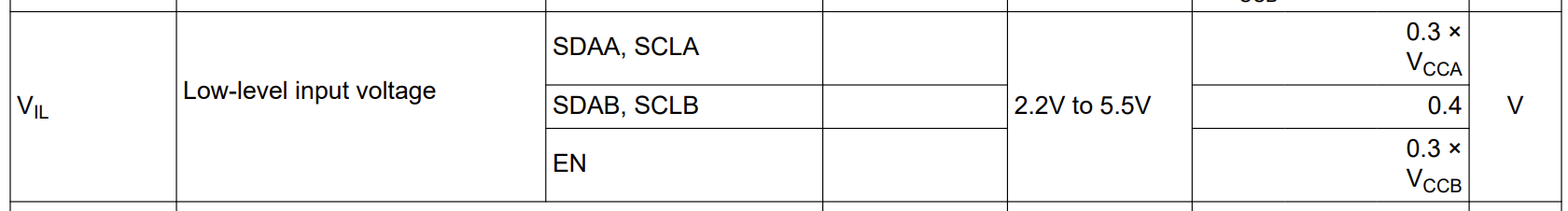
VIL or Low-Level Input Voltage
You might ask yourself, why is VOLB so large of a voltage output? It’s max is nearly 0.58 V on B-side regardless of the current output from the buffer? This is because the buffer needs to be a buffer — i.e. re-driving current from one side to the next, but also it needs to be bi-directional due to the nature of the I2C protocol.
Note that VIL for SDAB or SCLB is 0.4 V (max).
If you were to drive an input low signal on A-side, your output voltage on B-side is a max of 0.58 V. However, your input on B-side is 0.4 V. This means that if you drive a LOW signal below 0.4 V, you now drive the buffer in the opposite direction from B-side to A-side.
The TCA9617B has a buffered offset voltage of 0.58 V because it sets the output higher than its B-side input of 0.4 V. If the buffer were to output a voltage < 0.4 V, you could expect the buffer to lock up since its output re-drives back to its input.
Setting the buffered offset voltage to 0.58 V allows for some margin between the buffer’s output voltage and its input voltage. This allows the buffer to support bi-directional communication protocols, like I2C, where signals can be driven in both directions across the buffer. It does all of this without locking up.
Bi-directional buffer - TCA9617B