How Voltage Level Translation Works - LSF0102 - PCA9306
Voltage level translation, also known as level shifting, is a common electrical task that converts one logic level into another. For example, an MCU operating at 1.8 V may need to talk with a peripheral device that operates at a logic voltage of 3.3V. The MCU’s output high voltage (VOH) cannot go larger than its supply voltage of 1.8V, thus it can’t communicate a logic HIGH to the 3.3V peripheral. This is where level translation steps in.
The LSF0102 and PCA9306 device are two common passive level shifting devices.
LSF0102 is made for faster level shifting signaling working up to 100 MHz up translation and 100 MHz down translation for specified cap loads (characterized in the datasheet).
PCA9306 is similar to LSF0102 , but is made for I2C speeds up to 400 kHz. Practically speaking, both devices solve the same problem.
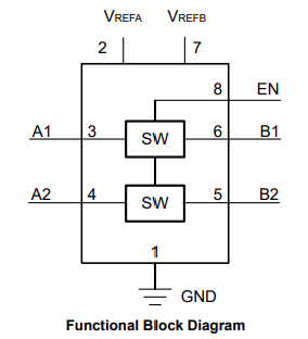
LSF0102 block diagram page 1/42 of the datasheet
Both level shifters can be used both as a level translating device or a switch. The difference in these two modes is dependent on voltage level and connection scheme f the device.
Voltage Translation Mode:
Voltage translation mode shorts the VREF2 (reference 2) and EN (enable) pins together. This helps to set the internal bias of the device to allow for level translation. The connection is pulled up through a 200k resistor to VCC2 which is the higher supply voltage. This is to limit current from VREF2 into VREF1 while also setting the proper bias at the VREF2+EN node.
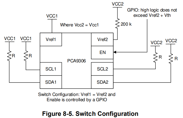
Page 13/38 of PCA9306 datasheet - Translation Configuration
Translation configuration for PCA9306 is limited to VCC2 >= VREF1 + 0.7 V. A voltage translation application of VCC1 = 1.8V and VCC2 = 3.3 V is very common here.
Switch Mode:
Switch mode is slightly different, but requires that VCC1 and VCC2 are the same voltage. The EN pin is controlled by an external GPIO, where the high logic voltage does not exceed VREF2 + VTH, where VTH is ~0.6V according to the datasheet.
Page 13/38 of PCA9306 datasheet - Switch Configuration
Switch configuration is helpful when the user wants complete control over the switch. Set the EN pin when you want data to pass through the device. GND the EN pin when you want the device to be a high-impedance path (PCA9306 is off). This can be useful if you don’t want the device to always pass a signal like in voltage translation mode. There is no control over the EN pin in voltage translation mode, so the device is always ready to level translate signals.
LSF0102 - Internal Circuitry:
Figure 7-1 from the LSF0102 datasheet describes the internal circuitry and how the EN pin biases the passFET’s connecting B1 to A1.
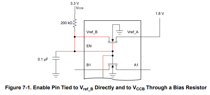
Page 10/42 of the LSF0102 datasheet - Internal Circuitry Diagram
VREFB is biased to VCCB = 3.3 V through a 200k pull-up resistor. VREF_B is shorted to the EN pin, and decoupled through a 0.1 uF capacitor to GND.
The EN pin connects directly to the gate of each passFET in the system. There exists a passFET between VREFB and VREFA. There is also a passFET between B1 and A1 as well as B2 and A2.
By connecting the EN and VREFB pins together, the passFET connecting the reference supply voltages looks like a diode where the anode (+) terminal connects to VREFB + EN, and the cathode (-) connects to VREFA. This connection scheme (voltage translation mode) sets the proper gate voltage of each passFET in the LSF0102 to approximately VREF_A + VTH, where VTH is the threshold voltage of the passFET (~0.6 V to 0.7 V).
LSF0102 Typical Application:
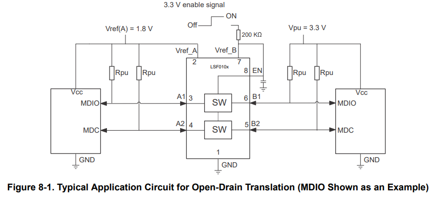
Page 12/42 of LSF0102 Datasheet - Typical Application Circuit for Open-Drain Translation (MDIO Shown as an Example)
The LSF0102 is setup in level translation mode where VREF(A) = 1.8 V and VPU = 3.3V.
When A1/A2 pulls LOW, current sinks from the 1.8 V through the open-drain driver of the MDIO / MDC signal. Current will also flow from VPU = 3.3 V through the pull-up resistor through the block labelled “SW.” In the pull LOW case, A1 follows B1, and A2 follows B2.
When A1/A2 releases HIGH, the pull-up resistors on both sides of the LSF0102 device pull-up to their respective voltage levels and the internal switch block (SW) becomes high-impedance. The MDIO Host sees 1.8V, and the MDIO target sees 3.3V in the idle HIGH state.